Electronics/LA3200: Difference between revisions
Created page with " == Documentation == Manuals can be found [http://www.ko4bb.com/getsimple/index.php?id=manuals here] just search for LA3200. According to [http://www.science-bbs.com/70-elec..." |
m add category |
||
| (17 intermediate revisions by 2 users not shown) | |||
| Line 1: | Line 1: | ||
[[Category:Tools_and_Equipment]] | |||
[[Category:Electronics]] | |||
{{Equipment | |||
| title = Logic Analyser | |||
| description = 32 channel | |||
| manufacturer = Thurlby Thandar Instruments | |||
| model = LA3200 | |||
| image = Thurlby LA3200 Logic Analyser.JPG | |||
| owner = Hackspace | |||
| induction = TBD | |||
| rfid = No | |||
| more_link = | |||
}} | |||
== The Basics == | |||
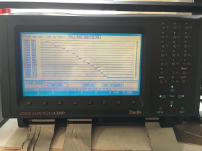
A logic analyser (analyzer) is used to probe digital signals in an electronic circuit. One example would be the digital input/output pins on a microprocessor such as an Arduino. The signals are displayed on a screen in the form of a timing diagram so that they can be compared against each other or against a timing reference. | |||
The logic analyser uses an external POD and cables to attach to the digital circuit. Different PODs are available for different functions. The POD we have is not an original part it was generated from the service manual. | |||
Requires the following improvements:- | |||
* Clock inputs need testing | |||
* 32 logic inputs proven to operate at low speed | |||
* 25 MHz operation needs testing | |||
* Enclosure needed for POD PCB | |||
Note that there is no input protection to the POD, therefore over-voltage may damage the POD. | |||
== Documentation == | == Documentation == | ||
| Line 16: | Line 44: | ||
(-) = link to | (-) = link to | ||
(*) = short together at pc end | (*) = short together at pc end | ||
The device is apparently identical to a Hitachi VC3120. | |||
Pod photos and even a PCB design for replacement pods can be found [http://www.eevblog.com/forum/chat/hitachi-denshi-logic-analyzer-vc-3120thurlby-la3200-pods-cabel-set/ here]. | |||
== Specification == | |||
[[File:LA3200 AP01 POD.JPG|150px|thumb|right|Logic Analyser with Pod AP01]] | |||
'''Logic Analyser''' | |||
* 32 channels (LA3200) | |||
* 25MHz synchronous operation on all channels | |||
* 100MHz asynchronous operation (8 or 12 channels) | |||
* 5ns glitch capture capability | |||
* Multi-level trigger sequencing | |||
* Non-volatile data and set-up memories | |||
* Disassembler options for popular uPs with specific PODs | |||
* POD AP01 for 32 channels | |||
[[File:AP01 POD RHversion top.JPG|150px|thumb|right|Logic Analyser Pod AP01]] | |||
'''Combination data pod AP01''' | |||
This is an assumed specification: | |||
* Obtained from ebay user robhookham, recreated from the service manual schematic | |||
* 32 data inputs (DC to 25MHz) | |||
* No 100MHz or glitch capture capability | |||
* No location for the disassembler ROM, this would need extra circuitry (TBD) | |||
* 3 clock inputs | |||
* 3 clock qualifier inputs | |||
* Input impedance 100k/5pF | |||
* Threshold TTL (1.4V) | |||
* Single 40-way connector with colour coded plug-on connection leads | |||
* The POD board's Eagle CAD files are available | |||
== Calibration == | |||
Not required | |||
== Induction == | |||
Ask on the mailing list for volunteers to demonstrate the use of any of the test equipment. | |||
==Basic Use== | |||
Only connect to 3.3v or 5v circuits. Higher or lower voltage may not operate correctly or may damage the AP01 Pod. | |||
There are weak internal pull-ups in the POD, therefore unconnected lines will be high. | |||
* Turn power on at the rear of the Logic Analyser | |||
* Select menu item via the button at the bottom of the screen | |||
* Either setup the analyser using menu item 1 or load a default setup from the store/recall menu item. | |||
* Select either timing diagram or state listing | |||
* You may wish to setup a trigger type | |||
* Press Run button on the bottom right | |||
* Select the type of analysis | |||
== Safety == | |||
[[Electronics/safety|You must read the safety documentation in this link before using this equipment.]] | |||
== Useful References == | |||
* | |||
Latest revision as of 11:06, 19 June 2017
 | |
| 32 channel | |
| Equipment Information | |
|---|---|
| Status | Unknown |
| Manufacturer | Thurlby Thandar Instruments |
| Model | LA3200 |
| Hackspace Information | |
| Induction Required | Yes |
| Induction Information | Here |
| Card RFID Enabled | No |
| Owner | Hackspace |
The Basics
A logic analyser (analyzer) is used to probe digital signals in an electronic circuit. One example would be the digital input/output pins on a microprocessor such as an Arduino. The signals are displayed on a screen in the form of a timing diagram so that they can be compared against each other or against a timing reference.
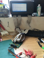
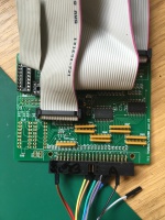
The logic analyser uses an external POD and cables to attach to the digital circuit. Different PODs are available for different functions. The POD we have is not an original part it was generated from the service manual.
Requires the following improvements:-
- Clock inputs need testing
- 32 logic inputs proven to operate at low speed
- 25 MHz operation needs testing
- Enclosure needed for POD PCB
Note that there is no input protection to the POD, therefore over-voltage may damage the POD.
Documentation
Manuals can be found here just search for LA3200.
According to this thread the pinout for the RS423 serial port on the back is:
2 - 3
3 - 2
4 *
5 - 5
6 *
7 - 8
8 - 7

(-) = link to
(*) = short together at pc end
The device is apparently identical to a Hitachi VC3120.
Pod photos and even a PCB design for replacement pods can be found here.
Specification

Logic Analyser
- 32 channels (LA3200)
- 25MHz synchronous operation on all channels
- 100MHz asynchronous operation (8 or 12 channels)
- 5ns glitch capture capability
- Multi-level trigger sequencing
- Non-volatile data and set-up memories
- Disassembler options for popular uPs with specific PODs
- POD AP01 for 32 channels

Combination data pod AP01
This is an assumed specification:
- Obtained from ebay user robhookham, recreated from the service manual schematic
- 32 data inputs (DC to 25MHz)
- No 100MHz or glitch capture capability
- No location for the disassembler ROM, this would need extra circuitry (TBD)
- 3 clock inputs
- 3 clock qualifier inputs
- Input impedance 100k/5pF
- Threshold TTL (1.4V)
- Single 40-way connector with colour coded plug-on connection leads
- The POD board's Eagle CAD files are available
Calibration
Not required
Induction
Ask on the mailing list for volunteers to demonstrate the use of any of the test equipment.
Basic Use
Only connect to 3.3v or 5v circuits. Higher or lower voltage may not operate correctly or may damage the AP01 Pod.
There are weak internal pull-ups in the POD, therefore unconnected lines will be high.
- Turn power on at the rear of the Logic Analyser
- Select menu item via the button at the bottom of the screen
- Either setup the analyser using menu item 1 or load a default setup from the store/recall menu item.
- Select either timing diagram or state listing
- You may wish to setup a trigger type
- Press Run button on the bottom right
- Select the type of analysis
Safety
You must read the safety documentation in this link before using this equipment.